Silicon Wafer

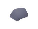
- Monocrystalline Silicon WaferMonocrystalline silicon wafer is one major type of silicon wafer that can convert sunlight into electricity. The other one is polycryatalline silicon wafer. When compared to polycryatalline silicon wafer, monocrystalline silicon wafer not only requires high purity raw materials,but also have relatively complicated production process.

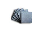
- Multicrystalline Silicon WaferMulticrystalline silicon wafer is the key material used for producing solar cells. They are widely used in photovoltaic power generation, communication, transportation and power supply to remote residential areas, and can also be applied to solar light, lawn lamp, rooftop solar photovoltaic power generation, and other areas.
Key components of integrated circuits of Silicon wafers, usually comes in two types. They are monocrystalline silicon wafers and multicrystalline silicon wafers. There are various sizes of silicon wafers available, and in particularly, diameter ranges from 25.4mm to 300mm. The thickness of silicon slice, systematically increases along with the diameter rising.
Silicon is widely considered to be the best material because wafer has adequate thickness to avoid cracking when handling. Silicon wafer, however, is not 100% pure silicon, they are always added into impurity dopant with an initial doping concentration between 1013 and 1016 at/cm3. Thus, they are classified as n-type or p-type depending on dopant and doping concentration.
The main procedures of silicon wafer fabrication are as followings:
1. Grinding process. We apply precise edge grinding machine to remove corner of silicon ingots.
2. Cutting process. The silicon ingots are cut into silicon slices accurately by coping saw into thickness of 120um.
Presently, we produce silicon wafer with thickness of up to 170um, thus our output rate is relatively high. Meanwhile, we are testing to apply 100um coping saw to cut silicon ingot, in order to reduce the waste of polycrystalline silicon.
We PV Company is leading professional silicon wafer manufacturer based in China. Through vast experience, we have obtained qualification for installing solar power station. In addition, we strictly control quality of our solar products according to ISO9001 quality management system. Thus, our products like silicon wafers, solar cells, and solar panel of solar modules, are certified by IEC, UL and CE. We also provide solar power solutions, solar product applications and research findings on 'Why Solar Energy'.
For further information on any of our solar products or for purchase, please do contact us !

 English
 Deutsch
 Español